Hello,so far there's two post about electronic that had been published so far.So,for this time it's all about ultiboard.What is ultiboard?It is a Rapidly prototype printed circuit boards (PCBs) with Ultiboard. The flexible Ultiboard design environment accelerates design with automated functionality while maintaining precision with manual control.
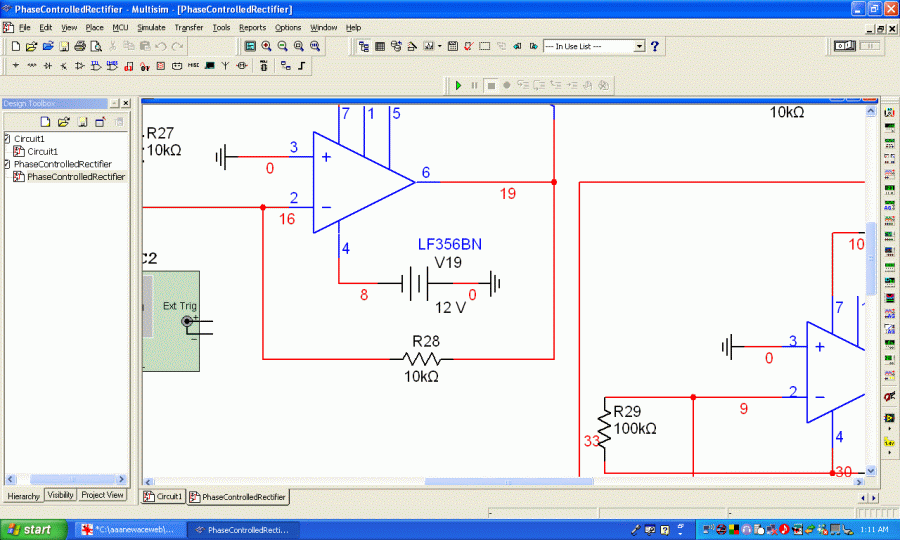
Circuit from multisim 11 :

Transfer to ultiboard :

3 Dimension version of ultiboard :

Procedure of using Ultiboard 11 :
1.Open the saved file from the mutisim 11
2.Transfer the schematic design to Ultiboard 10 by selecting Transfer » Transfer to Ultiboard 11.
3.Use the Save As dialog box to save the new Ultiboard file to your Z drive. Click
OK on the message box that appears.
4.Select the Layers tab near the middle of the left of the screen. This lists the board
layers and other useful elements of the board. Double-clicking a particular layer
sets that layer as active. Double-click Board Outline from the list.
5.Right-click an edge of the yellow rectangle and select Properties from the menu that appears. Under the Rectangle tab set the width to 2000 and the height to 1500. Click OK and notice that the yellow rectangle becomes much smaller. This rectangle represents the area of the circuit board in which all of the components and traces must fit.
6.Double-click the checkbox next to Ratsnest in the layers list. This removes the yellow lines that
connect all of the components together and simplifies the picture to lay the component.
7.Begin placing the components inside of the yellow rectangle. Notice single brown lines coming out of each component. These are Force Vectors and they point to the most efficient place to put the component based on its necessary connections. .Voltage limiter ideally have all of the components stacked on top of each other in the middle of the board.
8.The next step is setting the up the routing parameters for laying out the copper trace. Go to the Netlist Editor by selecting Tools » Netlist Editor. This tool keep track of all connections between pins on the board. Each set of pins connected together are referred to as a Net. Use the dropdown menu in the Netlist Editor to view the different Nets on the board. The tabs in the Netlist Editor provide different information and options for the selected net.
9.To prepare the Nets for routing select the first Net from the list. Select the Misctab and check the box next to Copper Bottom. This tells the Autorouter that this Net can be connected by placing trace either on the top of the board or the bottom of the board.
10.The board layout is ready for the Autorouter. Start the Autorouter by selecting Autoroute » Start/Resume Autorouting. The Autorouter should only take Possible Component Layout seconds to place traces for the board. Notice that there are green and red lines that appear. The green lines represent copper trace on the top layer of the board and red lines represent copper trace on the bottom layer of the board.
11.It is important to cleanup and check the work of the Autorouter after use. Excessive bends and sharp angles in the traces greatly increase the chances of board failure during manufacturing and use. Take some time to look through the traces and get a feel for dragging traces into more appropriate shapes and angles. The Autorouter is never perfect and there are always traces that can be cleaned up. Once you are satisfied with the traces on the board Save and Close the design.
So,I think thats all about ultiboard,more information will be updated later on.thank you.